- 您现在的位置:买卖IC网 > Sheet目录325 > FAN7083MX_GF085 (Fairchild Semiconductor)IC GATE DVR HI SIDE RESET 8-SOIC
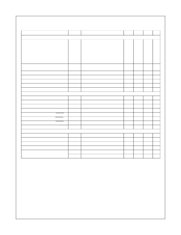
Statics Electrical Characteristics
Unless otherwise specified, -40°C <= Ta <= 125°C, V CC = 15V, V BS = 15V, V RESET = 5V, V S = 0V, R L = 50 ? , C L = 2.5nF.
Parameter
Symbol
Conditions
Min.
Typ.
Max. Unit
Vcc and VBS supply Characteristics
V CC and V BS supply under voltage
V CCUV+
-
-
9.0
9.8
V
positive going threshold
V BSUV+
V CC and V BS supply under voltage
V CCUV -
-
7.4
8.4
-
V
negative going threshold
V BSUV-
V CC and V BS supply under voltage hystere-
V CCUVH
-
0.2
0.6
-
V
sis
V BSUVH
Under voltage lockout response time
tduvcc
tduvbs
VCC: 10V-->7.3V or 7.3V-->10V
VBS: 10V-->7.3V or 7.3V-->10V
0.5
0.5
20
20
us
us
Offset supply leakage current
Quiescent V BS supply current
Quiescent Vcc supply current
Quiescent Vcc supply current
I LK
I QBS
I QCC1
I QCC2
V B =V S =600V
V IN =0, V RESET =5V
V IN =V RESET =0
V IN =15V, V RESET =0
-
-
-
-
-
50
65
75
50
100
140
160
uA
uA
uA
uA
Input Characteristics
High logic level input voltage for IN
V IH
-
0.63Vcc
-
V
Low logic level input voltage for IN
High logic level input current for IN
Low logic level input bias current for IN
High logic level input voltage for RESET
Low logic level input voltage for RESET
High logic level input current for RESET
Low logic level input bias current for RESET
V IL
I IN+
I IN-
V RIH
V RIL
I RIN+
I RIN-
-
V IN =15V
V IN =0
-
-
V RESET =5V
V RESET =0
-
-
-
3.0
-
-
-
-
15
0
-
-
5
0
0.4Vcc
50
1
-
1.4
30
1
V
uA
uA
V
V
uA
uA
Output characteristics
High level output voltage, V BIAS - VO
Low level output voltage, VO
Peak output source current
Peak output sink current
Equivalent output resistance
V OH
V OL
I O1+
I O1-
R OP
I O =0
I O =0
-
-
-
-
200
400
-
-
-
-
54
0.1
0.1
-
-
75
V
V
mA
mA
?
R ON
24
38
?
Note: The input parameter are referenced to COM. The VO and IO parameters are referenced to COM.
?2012 Fairchild Semiconductor Corporation
FAN7083_GF085 Rev. 1.0.1
4
www.fairchildsemi.com
发布紧急采购,3分钟左右您将得到回复。
相关PDF资料
FAN7085M_GF085
IC GATE DVR HI SIDE 8-SOIC
FAN7171MX_F085
IC GATE DVR HIGH SIDE 8-SOIC
FAN7190MX
IC GATE DVR HI/LOW SIDE 8-SOIC
FAN7340MX
IC DVR BOOST SW LED BKLT 16-SOIC
FAN7346MX
IC LED DRVR 4 CHAN BLU 28SOIC
FAN73611MX
IC GATE DVR HIGH SIDE 1CH 8-SOIC
FAN7361MX
IC GATE DRIVER HIGH SIDE 8SOIC
FAN7362MX
IC GATE DRIVER HIGH SIDE 8SOP
相关代理商/技术参数
FAN7085
制造商:FAIRCHILD 制造商全称:Fairchild Semiconductor 功能描述:High Side Gate Driver with Recharge FET
FAN7085_1
制造商:FAIRCHILD 制造商全称:Fairchild Semiconductor 功能描述:High Side Gate Driver with Recharge FET
FAN7085_12
制造商:FAIRCHILD 制造商全称:Fairchild Semiconductor 功能描述:High Side Gate Driver with Recharge FET
FAN7085_F085
制造商:FAIRCHILD 制造商全称:Fairchild Semiconductor 功能描述:High Side Gate Driver with Recharge FET
FAN7085CM
制造商:FAIRCHILD 制造商全称:Fairchild Semiconductor 功能描述:High Side Gate Driver with Recharge FET
FAN7085CM_F085
功能描述:功率驱动器IC MOS DRVR 300V 0.45A 1-Out Hi Inv RoHS:否 制造商:Micrel 产品:MOSFET Gate Drivers 类型:Low Cost High or Low Side MOSFET Driver 上升时间: 下降时间: 电源电压-最大:30 V 电源电压-最小:2.75 V 电源电流: 最大功率耗散: 最大工作温度:+ 85 C 安装风格:SMD/SMT 封装 / 箱体:SOIC-8 封装:Tube
FAN7085CMX
制造商:FAIRCHILD 制造商全称:Fairchild Semiconductor 功能描述:High Side Gate Driver with Recharge FET
FAN7085CMX_F085
功能描述:功率驱动器IC HIGH SIDE GATE DRIVER WITH RECHARGE RoHS:否 制造商:Micrel 产品:MOSFET Gate Drivers 类型:Low Cost High or Low Side MOSFET Driver 上升时间: 下降时间: 电源电压-最大:30 V 电源电压-最小:2.75 V 电源电流: 最大功率耗散: 最大工作温度:+ 85 C 安装风格:SMD/SMT 封装 / 箱体:SOIC-8 封装:Tube
